Speaker
Description
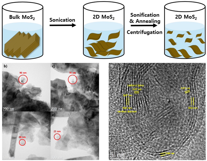
In recent semiconductor scaling, encountering physical limits, 2D materials are gaining significant attention. Among them, TMDs and MXenes are actively researched as 2D materials due to their superior electrical conductivity and physical stability compared to graphene. Among TMDs, MoS2 is bound by Van der Waals forces, allowing easy separation into individual sheets using sonification, and it has the advantage of being able to adjust the Bandgap according to the number of 2D layers. Furthermore, as MoS2 approaches 2D, it becomes mechanically flexible and exhibits a Direct Bandgap, with the advantage of a wider photoactive region compared to Si or GaAs. This study developed a radiation detector with an organic/inorganic hybrid active layer using MoS2 nanocrystals of various sizes obtained through ultrasonic exfoliation and centrifugal separation processes, as illustrated in Fig 1a. TEM images of MoS2 nanocrystals obtained at each rpm in Fig. 1b~e show that as the centrifugation speed increases, the size decreases. The TEM image of MoS2 nanocrystals obtained at 8000 rpm in Fig 1f confirms that even as the size decreases, the 2D characteristics of MoS2 nanocrystals are maintained.
The organic material used in the experiment is P3HT:PCBM, and to assess the effect of MoS2 size variations, the mixing ratio of MoS2 was fixed at 3 wt% for the experiments. Figure 2 shows the corresponding energy levels of the proposed detector and the process of charge collection.
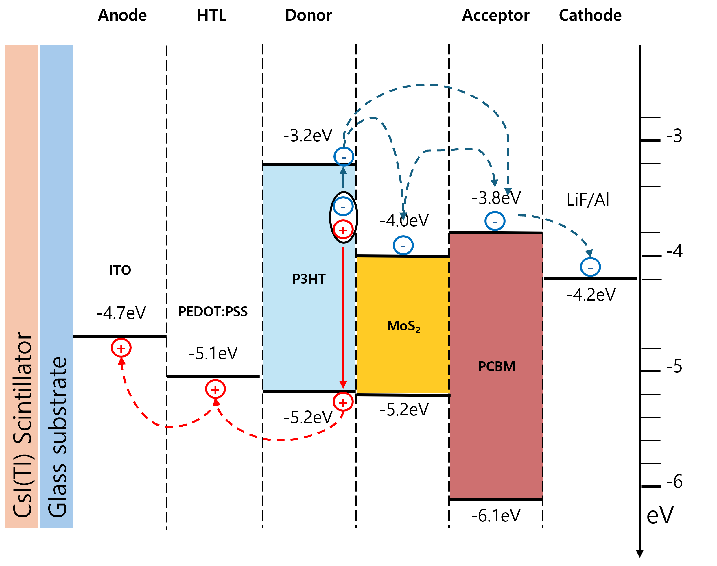
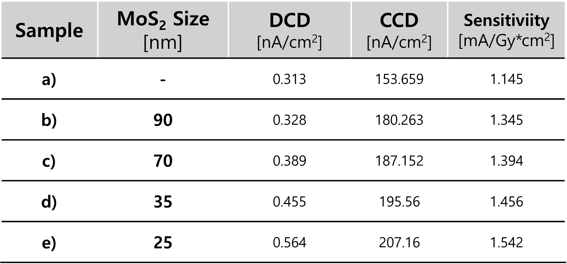
Fig 3 shows the parameters of the radiation detectors for samples according to the size of MoS2 used in active layer. The developed radiation detector demonstrates optimized results at 8000 rpm, showing a 34% improvement in sensitivity compared to detectors without MoS2 in the active layer.
Our results indicate that the use of 2D MoS2 nanocrystals is a promising approach to enhance the properties of semiconductor materials, suggesting its applications in a wide range of fields including electronics and optoelectronics engineeringemiconductor materials, suggesting its applications in a wide range of fields including electronics and optoelectronics engineering.